One of the major challenges faced by a patent licensing manager is to find and prove evidence of an infringement. Not so strong evidence of the use chart can become a standalone factor for the failure of a patent licensing program.
Reverse engineering can help confirm patent infringement by mapping relevant claims to the result of a product teardown. And a patent infringement can be confirmed when the publicly available literature has already been exhausted. To give you an example, we are sharing a case study where we helped our client prove patent infringement by using reverse engineering.
How we used Reverse Engineering to Prove Patent Infringement?
The task involved identifying the thickness of the substrate of a semiconductor device. In such a case, the availability of limited product literature is a common problem. Hence, we decided to go ahead with Reverse Engineering.
The task was to tear down a semiconductor chip in the connector of an Active Optical Cable. The chip had both optical structures, such as waveguides, and electronic structures, such as transistors, fabricated on the same wafer substrate.
The claim element – “a semiconductor wafer substrate having a region containing electronic devices, wherein the thickness of this region is in the range of 200-300 nm”, was difficult to identify in the online available literature. Therefore, teardown was the only way to confirm its presence in the chip.
In the first step, we identified the thickness of different regions in the product’s substrate. Let me show you what we got and how we used that to confirm the infringement.
Elements to be shown – a semiconductor wafer substrate having a region containing electronic devices, wherein the thickness of the region is in the range of 200-300 nm.
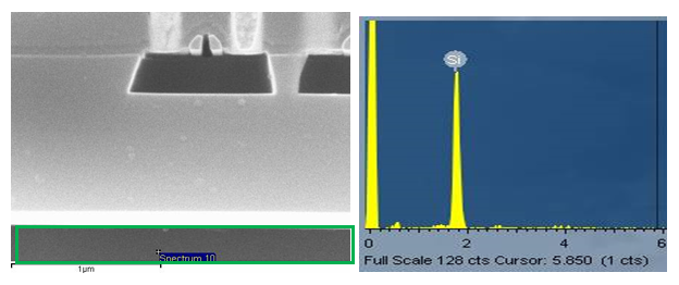
The green highlighted portion shows the base silicon layer. To confirm its presence, we performed chemical characterization using Energy Dispersive Spectroscopy (EDS) which indicated – right-hand side of the above image – that the portion contains silicon only.
Performing the same EDS analysis, we also confirmed a buried oxide layer in the base silicon layer shown by the green highlighted region of the above image.
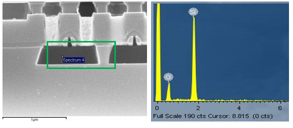
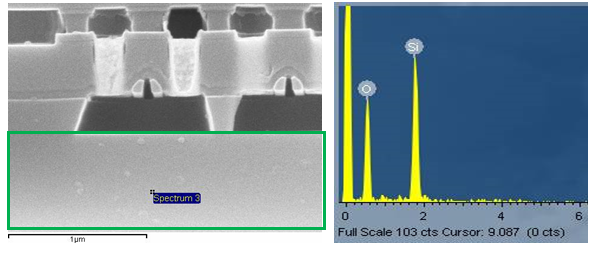
The highlighted portion of the above image shows the Epitaxial Silicon Layer present above the buried oxide layer. This made us conclude that the chip is built on an SOI (Silicon on Insulator) wafer as required by the subject patent.
Now the next task was to identify the region of the required thickness of the substrate.
Element to be shown – a semiconductor wafer substrate defining a region containing electronic devices, wherein the thickness of the region is in the range of 200-300 nm.
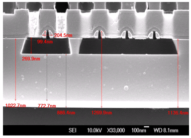
The thickness of the epitaxial silicon layer in the above image is 269.9 nm. This region had electronic components such as transistors embedded in it.
The analysis of the chip disclosed has a region that contained electronic components with a thickness in the range of 200 nm to 300 nm (i.e. 269.9 nm).
In a similar way, the studies can be performed on circuits, a flow of current, measurement, composition, etc. The whole idea being if there is a product that is using your technology we should be able to find it.
Authored By: Muzammil Hassan, Manager, Infringement Solutions.
Related Read: How we Performed Reverse engineering of an OLED Display to Confirm Infringement?