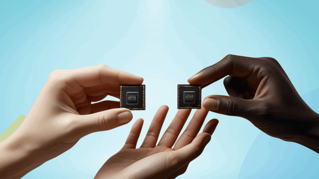
Did you know that an OLED is 200 times thinner than a strand of a human hair? The thickness of a strand of human hair is approximately 30 to 100 micrometers while that of an OLED is 100 to 500 nanometers. Pretty thin, eh?
Well, the story I am about to share with you today is about confirming infringement when there is not enough information available. It is about dissecting this super-thin OLED screen to look inside it and figure out how it works. This process, also known as reverse engineering (RE), can play a crucial role in detecting and proving infringement.

The RE – which was an aftermath of a patent infringement analysis we worked on for one of our clients – was unsurprisingly challenging. Before I dive into its details, let me give you a glimpse of the situation we were facing.
Mark, one of our old clients, wanted to identify the potential of an OLED patent (US’938) from his client’s portfolio. His ultimate objective was to sell the patent. Considering OLEDs are a hot topic with companies trying to research, develop, acquire and sell the technology; if the infringement could be proved, this patent would fetch a good amount.
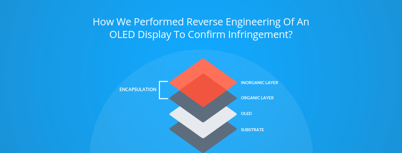
As soon as we got the email from Mark’s side, my team started the detailed infringement analysis of US’938 which was related to encapsulation layers used in OLED. This layer covers the OLED and acts as a barrier to protect OLED from moisture penetration.
Two roads diverged in the research and – I took the one less traveled by….
Our initial research revealed that OLED Display Inc. — a consumer electronics giant and one of the biggest manufacturers of OLED — uses encapsulation layers.
However, after an extended search, we figured that the product literature did not cover sufficient details related to the composition of layers or their arrangement, so overlap could not be confirmed.
Next, we studied the research papers and patent filings by OLED Display Inc. (Will be referred to as ODI from henceforth for brevity) to understand the technology behind its encapsulation layers. This is not the perfect way, but it gives a good idea of what researchers inside the company were thinking.
During the search, we found a patent application (US’355) of ODI covering the invention described in the US’938. This was a positive lead indicating that the products of ODI might overlap US’938 patent.
This was the point where the two roads diverged, and we suggested to Mark – “Let’s walk on the less traveled road of Reverse Engineering.”. Since the lead was promising he gave us an approval to start the work on it.
Since ODI is a top player in displays, a patent overlapping its flagship products would drastically increase its value. The road was leading to fulfilling Mark’s objective to tap the potential of the patent. Considering this, we looked into the possibility of acquiring the OLED display from the market and then reverse engineering it to identify the necessary details on encapsulation.
And Then Came the Battle Field Analysis…
Keeping Mark in the loop, we evaluated what tests could be performed on the display. Next, we had to select an OLED by ODI to dissect and peek inside.
We had to pick the right display in the very first go. The situation was similar to the movie scenes where a protagonist diffuses a bomb. Green wire, yellow wire, red wire – which one to cut!
Cutting the right wire — cool. Wrong one—boom! We didn’t want a boom. So, we took multiple factors into account for the RE. Some of them were:
- The feasibility of performing RE
- Hurdles that we may come across
- Tests required confirming each claim element, steps involved, and their feasibility.
After multiple brainstorming sessions, we decided to go ahead with the OLED of one of the flagship products of the electronics giant. We worked out the plan with Mark and we were all set.
And here began my journey to find a strange footprint on the shores of the unknown….
Unknown is something that frightens everyone. But the unknown is where we find crucial answers to our prudent questions. And as Stephen King says, “It’s the unanswered questions that make it worth getting up in the morning.”
When I began with the RE on that morning, I felt like a kid at Christmas. And the kid inside me couldn’t sit still. I was curious to see what was behind the encapsulation technology used by ODI. I would get the answers to what we tried looking for through digital research.
Getting to know unknown would take some effort. So we prepared for the same. A significant part of it was the collaboration with a semiconductor lab to carry out testing. First, the team and I worked remotely with lab assistants. Later, I flew 2585 miles to the Semiconductor lab in our other office for carrying out the tests.
Before I share how our cart moved on the roller coaster, let me first give you a quick run-down of the major steps of the geeky-process which were:
- Sample preparation – Disassembling, cutting, grinding and FIB milling of the sample.
- Tests for Imaging Semiconductor Layers in Display – Scanning Electron Microscopy (SEM), Transmission Electron Microscopy (TEM)
- Test for analyzing Composition of Semiconductor layers in Display – Energy Dispersive X-Ray Analysis (EDX)
We started with the first step of Sample Preparation. And I could sense the excitement building inside me like a fizzy soda drink.
I could picture it already – holding the sample in my hands. It was giving me a jolt of tingling feelings. Then I would take it for SEM, TEM and other tests. I could see everything. It seemed so natural and flawless.
However, as they say – we suffer more in imagination or due to it. The excitement was short-lived. It escaped so fast like Helium escapes Earth’s atmosphere. You might have seen it coming—we weren’t able to prepare the sample within the first attempt, nor the second or the third.
The 5th time, however, was the charm. The sample was extremely sensitive to temperature, which is why it took us multiple iterations to get it right.
In each iteration, the temperature was lowered than the previous one. To top it off, each iteration was damaging our sample due to temperature exposure.
Well, truth to be told, I didn’t anticipate this at the outset. At that moment, I remembered that this is part of walking on an unknown road. It was time to make wrong right again, and act with a cool head and patience of a military sniper.
As we were continuously lowering temperature previously, I had some data to act on. After the trial and errors, now was the time to get it right.
And this time I hit the home run.
I had the right sample ready for testing. Looking at it was similar to sipping water after a steep uphill climb. I could feel a drop sliding down the food pipe—a sliding drop of hope.
Good, Better, Best. Never let it Rest!
After preparing the sample, I had already gained some inertia and I wanted to keep going. There is no stopping from here is what I had in mind.
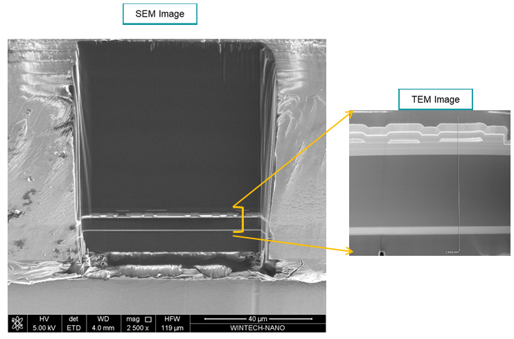
The next objective of the testing was to identify Encapsulation layers in the OLED and then analyze its composition. Since we were dealing at the nanometer level, we pursued with specific tests like Scanning Electron Microscopy (SEM), and Transmission Electron Microscopy (TEM).
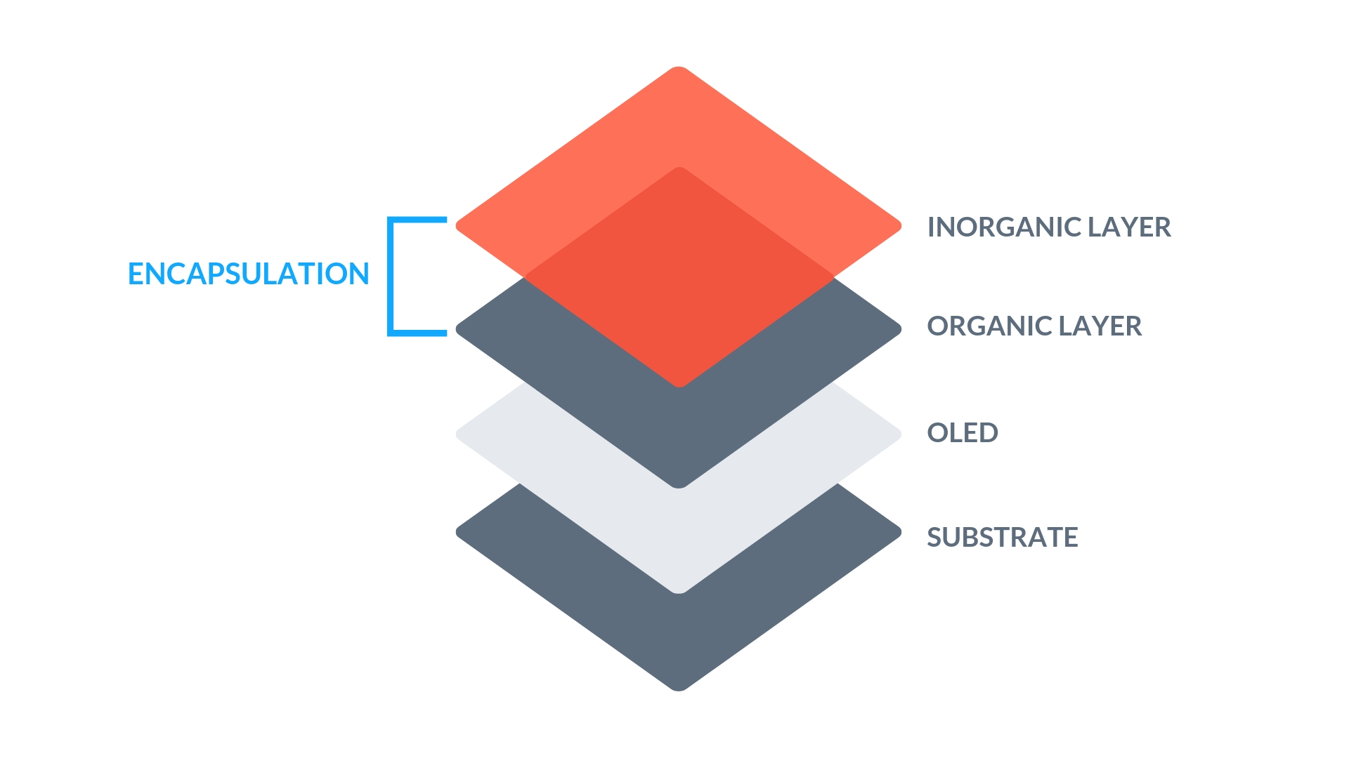
In the first go of SEM, we took specific images of the layers in the sample and identified their composition through EDX.
Now, the next objective was to identify one of the holes – the encapsulation layers.
During the digital analysis, we had prepared a database of materials which are commonly used for each layer present in an OLED.
So once we had the SEM scan, we compared each layer against the database and tried to conclude which layer is which – for example, we identified the substrate where carbon content is high and present at the bottom-most area.
This was the first bump where I lost some of the gained inertia. We could not spot any layer in the scan matching with the encapsulation layer in our database. Yes, another note from the melodies of sad coincidences.
My thoughts danced in all directions of the three-dimensional plane. If time is the fourth dimension, then they danced there as well. All I thought was – Why?, and what could I do next?
One thought then emerged as the sun on a rainy afternoon. We thought it could be the case that the image resolution wasn’t high enough to show the encapsulation layer.
So we had to get a high-res image. Yes, that’s it. And We had TEM for that. SEM offers 2 million magnification level while TEM offers a whopping 50 million!
We repeated the process with TEM while my psychological exoskeleton was trying to wither the thought what if this fails as well. The same process of comparing against database was executed. We had a high-res image, but there was no encapsulation. It felt like spotting a dried well in Sahara desert.
When the going gets tough, the tough get going
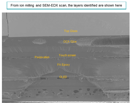
I started wondering – How could this be possible? The expected position of encapsulation is on the uppermost side of the sample. But, during testing, the uppermost layer came out to be a cathode and there was no encapsulation layer.
This finding was in contrast to the digital literature as in every document, the presence of encapsulation is supported.
The beauty of science is that it works. And if it works once, under the same conditions, it works umpteenth times. So, I decided to keep the ball rolling. Because if literature confirms, the layer should be where it meant to be.
On an analysis of where I could have gone wrong, I decided to take more scans from different angles.
I repeated the analysis about 20 more times taking the scans from different angles, repeating the match process, studying each time in more depth, referring research papers, digging more and more each time, but to no avail.
Every time the output was the exact opposite of what was given in the product’s literature. At this time, the failure started growing on my thoughts. Has the fear of unknown manifested itself as a thought of being a failure, I questioned myself?
There were a few ups and lots of downs during the analysis. However, something in me was telling me that the ride hasn’t ended yet. I was doing science. If it worked once, it will work again.
What to do next, what to do next, what to do next? Should I prepare another sample? Was the temperature an issue? Should I try with another angle? Truth to be told, a glorious firework of questions was going on my head similar to the one you could spot on the night of 4th of July.
I essentially threw spaghetti of questions at the wall of my frontal lobe. And one question stuck. I decided to contact the experts of the OLED.
I reached out to numerous experts involved in research of semiconductor manufacturing, professors, authors of OLED research papers, etc. I tried explaining my situation, the process I followed, and discussed why the encapsulation layer is not available. I got a few answers; some of them even seemed reasonable.
Unfortunately, the answers did not work in our case.
Rest you must but don’t you quit!
I realized that I had hit a brick wall. I think I’m not alone – you must have encountered the same feeling – we have all been there. It feels there is no way out.
The next moment, my brain took me on a ride to the alley of similar past experiences. There were posters glued on walls screaming mutely with enthusiasm: there was a way, and I found it!
I gave the status update to Mark – well, all this while he was kept posted – and explained where I was stuck. Mark is very co-operative and he understood the situation.
Mark had given us flexibility and it comes with a responsibility. A responsibility to not let the giver down. And that’s what I was thinking about Mark. I had to find the way that leads to glory.
Amidst all this, I already had a holiday planned with family – I got married recently – and had to fly back to India for holidays.
But the vacation didn’t take the thought of finding the way out of my head. I was obsessed about it. Nevertheless, the vacation offered me time to reflect, and rejuvenate.
One night, I was doing an audit mentally of everything that happened and began questioning – where I could have gone wrong, what I could have left unturned, and what else I’m missing?
I was able to zero-in and came up with few pointers. One of the pointers was to contact an expert. While I was working in the lab, I came to know about an expert working remotely.
I connected with the expert through emails. In the next few exchanges, I explained to him multiple aspects of the tests. From the discussion, I figured that sample preparation needs some alterations if I wanted to look into the encapsulation layers.
After an entire ordeal, I finally knew where the key to the labyrinth lied.
And the light at the end of the tunnel revealed the finish line…..
When I went back to the lab, I felt the same excitement I felt during the start. And history repeated itself. This time it wasn’t a bump on the road, but a pothole.
The product sample that we procured could not be reused now because it was damaged due to the earlier tests.
We procured a fresh sample, which took its own sweet time to arrive and performed the test again. This time preparing the sample in an alternative way, as suggested by the expert.
With this round of testing, I was able to connect the dots. I could see the encapsulation layer on the top, and EDX showed the composition of the layers as required. Finally, all the pieces fell into place.
Confirming Infringement
Completing the Reverse-engineering was certainly a hard nut to crack. Though we were successful in reverse-engineering the display; however, the findings didn’t make us happy.
The objective was to confirm infringement with US’938. By analyzing the patent details and output from reverse engineering, it was concluded that the flagship smartphone’s display encapsulation layers did not have the same composition as claimed in the patent. Hence, it wasn’t infringing.
However, I was okay with the outcome, because I knew we left no stone unturned in the process of finding out whether there was any overlap. Moreover, I got answers to what I was looking for – composition of encapsulation layers.
Throughout the process, we kept Mark informed of the happenings. Every minor observation was shared via quick emails to keep him on the same page all the while. Mark knew:
- When we were stuck at sample preparation,
- When we could not identify the encapsulation layer,
- And our next course of action.
After we concluded that there is no infringement, we prepared a document showing our analysis and output from RE. This document was shared with Mark and his client. We discussed the process and outcome in detail over a call with Mark and his client. Though the outcome was not as expected, we still received positive feedback from Mark.
The whole project was full of learning. It matters a lot how you reach your goal. I was able to find answers in this case only because I was sticking to my guns. Many a time, I did not anticipate the hurdles involved in every small step and tripped right over them. But the persistence finally paid off.
When it comes to infringement searches, it often happens that the outcome is not fruitful, but we still saw clients coming back to us for their next project, because at GreyB it is in our DNA to keep trying until we find the results. We simply do not go on to claim – “If it exists, we will find it.” We stand by our words, every single day, not just because we want to become the best search vendor, but because we believe in helping our clients reach their goal, as any good partner would do.
Authored by: Vincy Khandpur, Team Lead, Infringement.