Patent filing in the semiconductor industry has exploded in recent years as new technologies like the internet of things, machine learning, and artificial intelligence have rapidly expanded in the chip market. There are an estimated 50 billion connected devices globally, according to Ericsson. Chips are no longer the preserve of mobile phones, but can also be found in cars, appliances, medical equipment, and more.
This has made it extremely difficult for semiconductor and electronics companies to understand whether their IP is being used without their knowledge. Patent technologies are smartly sneaked, amended, and granted again. It needs more cleverness to invalidate such patents (look like novels but are not) and we at GreyB have done that multiple times. Each time it requires a new strategy, a different thought process, multidimensional analysis, keen observation, and a lot of exploration.
How do we go about invalidating such patents? Lemme tell you all about it right after we have a look at some insights about filing and litigation in the patents related to semiconductors.
What do filing and litigation trends in the semiconductor domain look like?
We analyzed the patent publication of two patent offices – USPTO and EPO and here’s what we found.
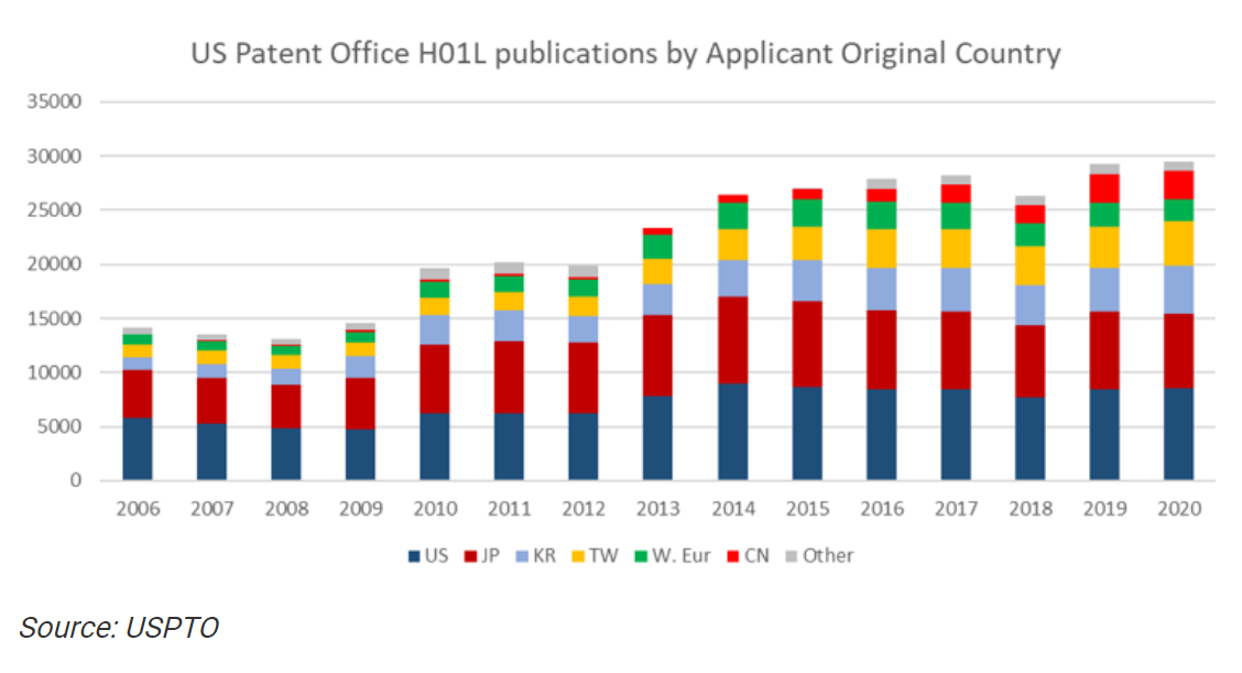
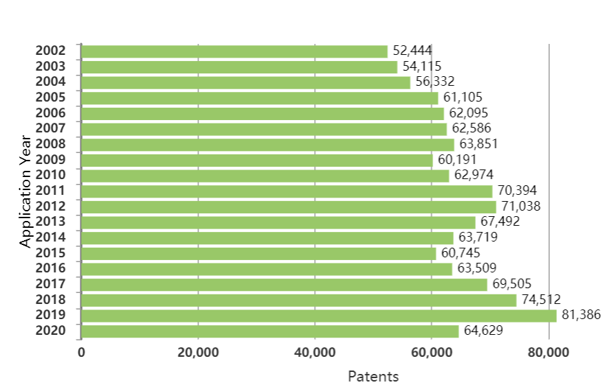
The USPTO has the most publications associated with H01L, a technology class code used as a proxy to identify semiconductor-related patents, with nearly 30,000 in 2020. During the period of 15 years studied, we found that the number of publications at the USPTO increased at a 5.4% average annual growth rate.
The below chart depicts the number of semiconductor patents filed from 2006-2020.
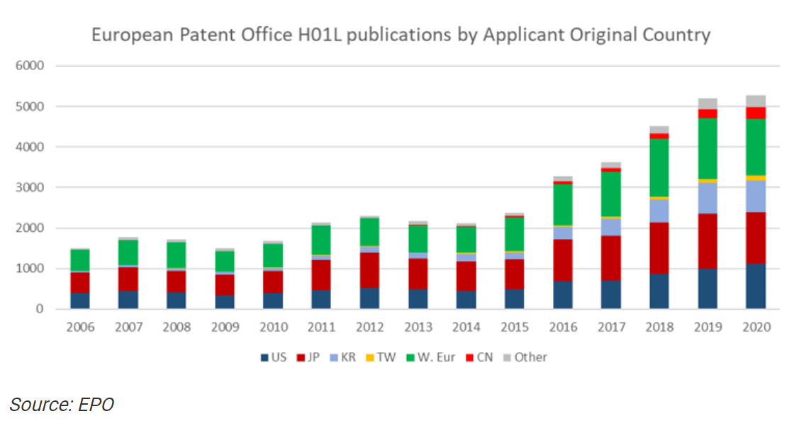
Over the 15-year time period, the number of H01L-associated patents published by the European Patent Office (EPO) increased at an average annual rate of 9.4% (see figure 2). Much of this growth started around 2015 with the rate from 2015 to 2020 sitting closer to 17%. The image below should help paint a clearer picture.
As we can see the overall application filed in the semiconductor industry has been continuously increasing.
With the increase in the investment in R&D from a lot of companies in this domain – it is natural for industry participants to engage in actions necessary to protect the inventions and technological advances produced by those efforts.
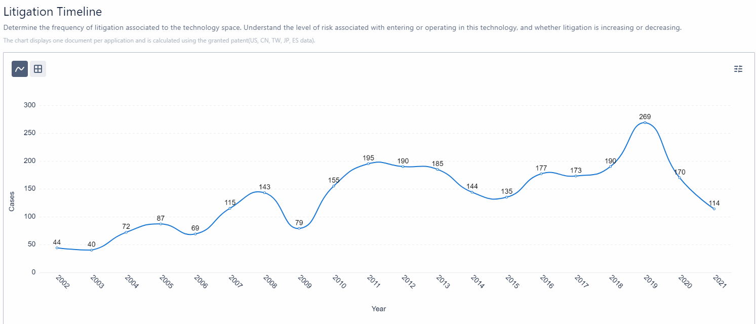
With every passing year, the number of invalidation cases or IPR petitions filed has risen like never before. Around 1600 patents are still in litigation.
The graph below depicts the increase in the number of litigation in the domain.
If you’re working in this domain, how do you respond to such litigations? Of course, you would want to invalidate them. But these patents are not super easy to invalidate. So I have next shared some well-tested techniques/methods, which you can peruse to invalidate semiconductor-related patents.
These hacks can help you invalidate semiconductor patents
-
How the patent is granted using the combination of prior-arts
As we know that the semiconductor is continuously growing since 1940 so are the technologies related to it. It can be very easy for someone to merge two existing technologies and get a patent. For example-
If a dipole antenna is designed on a substrate, incorporation of a low pass filter with the pre-existing circuitry can help in lowering the common-mode resonance because the current will bypass through the low pass filter. Anyone knowing this domain can understand that. For more clarity, please refer to the basic circuits of the dipole antenna and antenna structure.
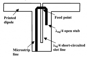
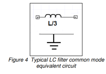
Now let’s say there is a concept (like the below figure) where sorting line 20 having an inductor (low pass circuit) is added to the basic circuit of the antenna to eliminate the common-mode resonance (by passing low-frequency currents from sorted line 12).
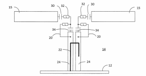
One can simply see, it is nothing but the combination of the above two concepts which would be very obvious for any person.
Similarly, if a substrate is designed to absorb more heat and another substrate is designed to make faster transmission then it is obvious that a substrate having both the qualities can be prepared (not invented).
-
Same circuit/design solving multiple problems leads to granting of multiple patents
The addition of elements in pre-existing arts may solve several problems thus multiple patents can be granted. As in-
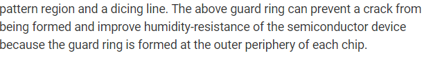
Implementing a seal ring outside the circuit may be intended to prevent the wafer from the cracks, but it also provides temperature stability and protection from humidity and rigidness. Someone making minor changes in the seal ring can get a patent explaining other mentioned industrial applicability.
Let’s understand this with the help of an example-
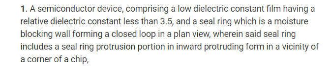
In the US20110215447, a seal ring is intended to protect the wafer from moisture. Below are the claim and image of seal ring 123.
We invalidated such a patent with a seal ring which was almost of the same material but majorly targeting the crack prevention in the wafer. But somewhere, it was written that it additionally can save the wafer from humidity too. Please see the reference given below.
These types of patents can be invalidated after research about the added element like its material, its characteristics, and multiple industrial applicability.
-
Observing elements and their significance
Keen observation of the claim elements and the functions performed by them is necessary for semiconductor patents. The ordinary element performing the same function can be used to invalidate the patent. We can understand this with the help of the below examples-
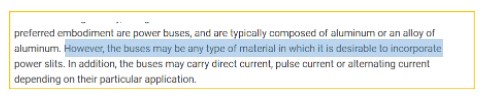
In the recent invalidation case we got, the patent claimed a very specific portion of a substrate which further included a power bus made of aluminium.
If we look at this, any conductive layer which is used for power transmission can be inferred as a power bus. We found the same wafer design but with the copper power bus. We invalidated this patent with a power bus made of copper only because it was performing the same task. The scope of the claim was also quite broad. Below is the snapshot of the text which helped us in invalidating the claims.
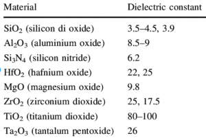
Another scenario is often, the claim limitations are woven around the dielectric layer. So, unless its scope has been limited to a particular material, any layer made of ceramic, plastic mica, Glass, etc. at the same place can be considered as the dielectric layer. The below image shows the multiple materials that can be used as a dielectric layer.
-
Dimensional claim restrictions can be invalidated by standard range theories
Sometimes the restrictions related to dimensions are claimed in the subject patent. To invalidate this, we believe standard literature like checking if the dimensions are in the standard range or not can prove very fruitful. We observed that the reason for this is normally standard literature elaborates the concept in quite detail and from all possible perspectives including the ranges.
Let me elaborate with an example.
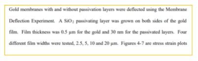
Once we got an invalidation in which multiple thicknesses (1,2,3 micrometer) of passivation layer were claimed. We presented an NPL with the below text, to invalidate the same-
 Similarly, we always plan to go through semiconductor standards like IEC 62258 and industrial standards like SEMI 1910.124 to invalidate the semiconductor patents claiming numerical and standard amended information.
Conclusion
Overall, the Semicon domain is progressing at a never-before rate. With that, the litigation trend is definitely going to take a steep curve.
Also since most of the tech (as per our observations) is not actually novel. They are likely either a borrowed concept or a combination of two ideas. The above strategies/hacks can definitely come in handy to challenge these types of patents.
We agree with the quote-
“Semiconductors are becoming ubiquitous,” – Gavin Carter
Adding to this, we believe that “Semiconductor replicas are becoming ubiquitous” and we are open to prove that.
Subscribe to our blog and never miss another update on the Semicon Industry.
Authored By: Ajay Kumar, Prior art team