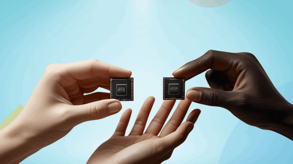
Recently, one of our client contacted us with a project which required a Reverse Engineering based infringement analysis of cutting edge tech. This article discusses how we went about the RE and helped monetize the patent portfolio.
A few months ago, we were contacted by Bob*, VP of IP Monetization at a Fortune 500 organization. Bob needed our help in monetizing a big chunk of their patent portfolio using Reverse Engineering based infringement analysis.
This portfolio was related to cutting-edge tech – with patents on various technologies, ranging from semiconductor fabrication techniques to complex communication systems, and transistor-level circuit analysis to system analyzing through signal analysis.
Bob shared that he ignored these patents as earlier infringement searches lead to no conclusive evidence of use. We performed a first pass of the patents and were able to share a few examples of how the shortcomings of online searches can be overcome using Reverse Engineering.
We walked Bob through some of our ideas backed with logic and Bob decided to bank on us and gave the few patents from the under-monetized portfolio another chance.
Today, in our brief time together, I would like to share how we proceeded with a RE of one of these patents.

We conducted a reverse engineering analysis to understand the various processes happening inside a smartphone. Here’s how we did it.
For starters, we did a signal analysis to reverse engineer the various processes happening inside a smartphone.
For this project, our objective was to identify the sequence of operation for various processes that are happening within a smartphone. Now, this type of information (related to specific signals) is generally not discussed in the product literature available online.
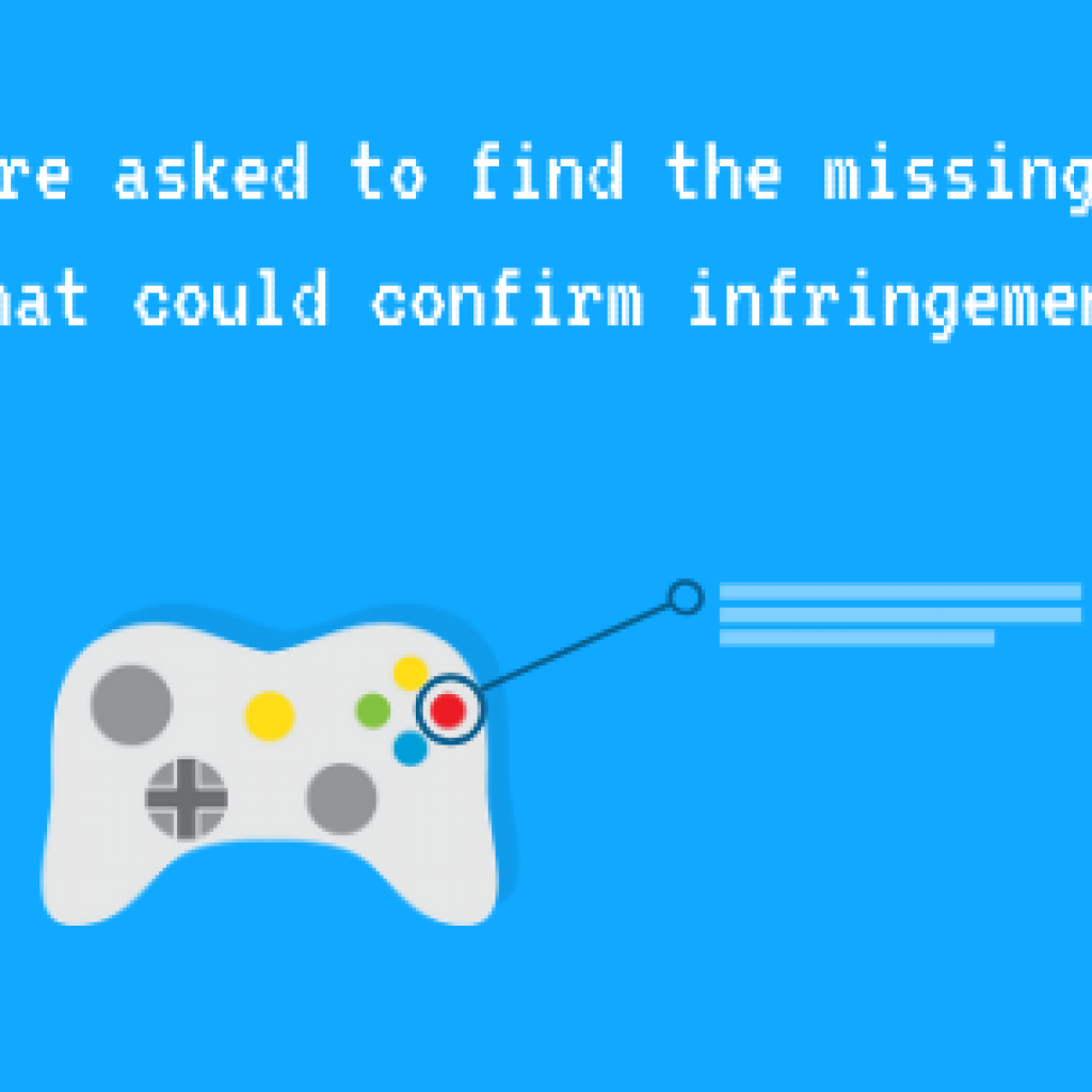
The claim element of the patent under focus – “activating the fingerprint sensor and subsequently, performing data communication from the fingerprint sensor”, was difficult to identify in the online available literature too. Teardown, and signal testing, thus, was the only way left to confirm this step in the functioning of the smartphone.
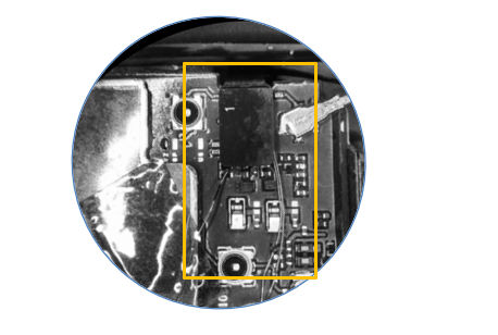
To analyze the fingerprint signals from the sensor, we had to first tear down the target smartphone to expose the various points on its motherboard. Exposing these points was required to enable the measurement from these points.
A caution point – While doing reverse engineering we had to make sure that the phone is in working condition so that we can test the fingerprint functionality.
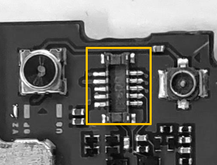
Zoomed-In Image: Motherboard of Target Smartphone Showing the Identified Connector for Fingerprint Sensor
After identifying the connector on the motherboard of the smartphone to which the fingerprint sensor is connected, we soldered the jumper wires to the points of interest using micro-soldering process, so that we could connect them to the probes for taking the readings.
 Zoomed-In Image: Motherboard of Target Smartphone Showing Soldered Jumper Wire on The Identified Connector for Fingerprint Sensor
We used a mixed-signal oscilloscope (MSO) for taking the readings. The reason for picking an MSO was to get the visual timing diagram for the various signals within the smartphone.
We were ready for taking the readings at this stage. But, this type of testing demands one more crucial step i.e. building-up an exhaustive list of testing scenarios. This exhaustive list not only should contain all the related scenarios, but it should contain all the possible scenarios including the random tests.
Once all the test cases were prepared, we started executed them one after the other.
Elements to be shown – “activating the fingerprint sensor and subsequently, performing data communication from the fingerprint sensor”
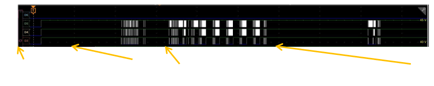
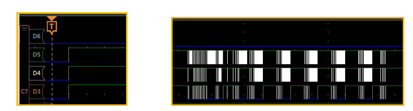 Timing Diagram from the MSO
We then collated all the test cases to study how the phone was working internally. For example, if we look at the timing diagram from the oscilloscope, it provided the piece of evidence that the fingerprint sensor is first activated, and then at a later stage, the data communication from the fingerprint sensor takes place. The various test cases taken at different testing scenarios showed the same sequence. This helped us build the case.
Using these pieces of evidence and more information from our analysis, we prepared the claim charts that later helped Bob build a strong case.
Conclusion
Not all patent infringement analyses are created equal. Some analysis could be done using a detailed web search where one explores product manuals and other relevant literature. While in some, one might need to take the reverse engineering route to confirm patent infringement.
Further, Reverse Engineering doesn’t just involve testing the outer screens of smartphones. Some require teardown of the circuits to determine the flow of current, measurement, composition, etc. The whole idea is – if there is a product using your technology, you should try to find out the evidence, and start a new revenue stream from your business.
Does your portfolio have patents that you feel are being infringed by other companies, but the past search wasn’t successful? Rohit and I think would be curious to look at your portfolio and share if there is an alternate way to identify evidence. If you want to discuss more, we would love to chat with you.
Let’s chat.

Authored By: Swapnajeet Nayak, Senior Research Analyst, Infringement and Rohit Sood, Manager, Infringement