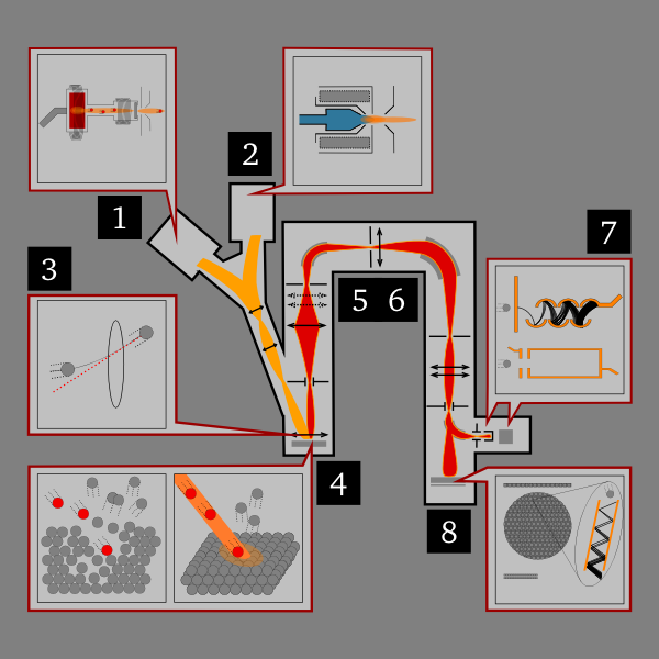
Dynamic SIMS
- Dynamic Secondary Ion Mass Spectrometry instruments capable of parts-per-billion sensitivity for depth profiling analysis.
- Has high mass resolution capability, and often used for P doped samples in SI wafers (MR > 4000).
- Depth profiling can be optimized for low energy ultra-shallow implants or for several micron deep layers
Specifications
- Dual source (O & Cs)
- Sensitivity: ppm-ppb
- Depth resolution < 1nm
- Detect all elements with isotope information
- Sputter energy: O 2+: 1-10kv, Cs+: 1-15kv
- Best mass resolution > 25400
Applications
- Depth profiling
- Thin film composition: Ntrided gate oxide and SiGe
- Contamination analysis and control in oxide/active/well
TOF SIMS
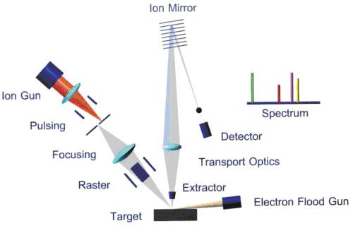
- Time-of-flight Secondary Ion Mass Spectrometry is a versatile instrument capable of parts-per-million sensitivity or better with parallel detection for nearly all elements and molecules up to several thousand atomic mass units.
- Mass resolved imaging provides mapping with lateral resolution better than 150nm.
- Surface analysis sensitivity is comparable to TXRF, though it also provides lower mass range sensitivity and targeting of smaller areas.
- Depth profiling with sputter ion guns can be optimized for low energy ultra-shallow implants or for several micron deep layers.
Specifications
- Mass range: 0-10,000 amu
- High mass resolution: M/ΔM over 10000
- Sensitivity: ppm-ppb
- Detected element: H – U (Isotope)
- Depth resolution: <1 nm
- Lateral resolution: 0.1-1 µm
- Sputter gun: O2+: 0.25-2kv, Cs+: 0.25-2kv
- Analysis gun: Bi+, 25kv
Applications
- Surface analysis of organic and inorganic materials
- Elemental and molecular information about surface, thin layer, interfaces of material and surface contamination
- Positive & negative ion mass spectra and 2-D ion mass spectral image information
- 3-D ion image analysis
- Depth profile analysis
XPS (X-ray Photoelectron Spectroscopy)
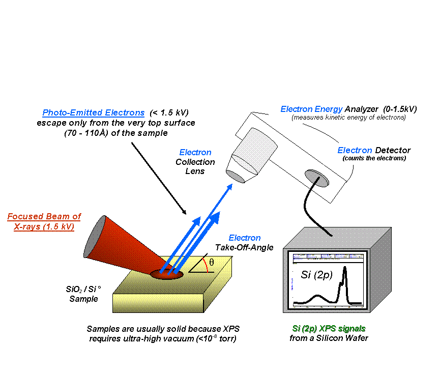
- X-ray Photoelectron Spectroscopy is qualitative surface analysis technique that can characterize the surface chemistry of materials (chemical state and concentration).
- X-rays are focused onto material, and then measure the emitted electrons intensity and energy from the top 1-10nm of the surface.
- Quantified elemental depth profiling through layers can provide both layer and contamination intensities.
Specifications
- Beam size: 7.5-200 um
- Lateral resolution: 10 µm
- Depth resolution: 1.0 nm
- Energy resolution: 0.48 eV
- Detected element: Li – U
- Sensitivity: 0.1-1.0 at%
Applications
- Surface analysis of inorganic and organic materials, contamination, stains or residues
- Quantification of surface elemental composition
- Determination of chemical state/bonding information
- Depth profiling for thin film/material composition
- Film/material and oxide thickness measurement
FTIR (Fourier Transform Infrared Spectroscopy)
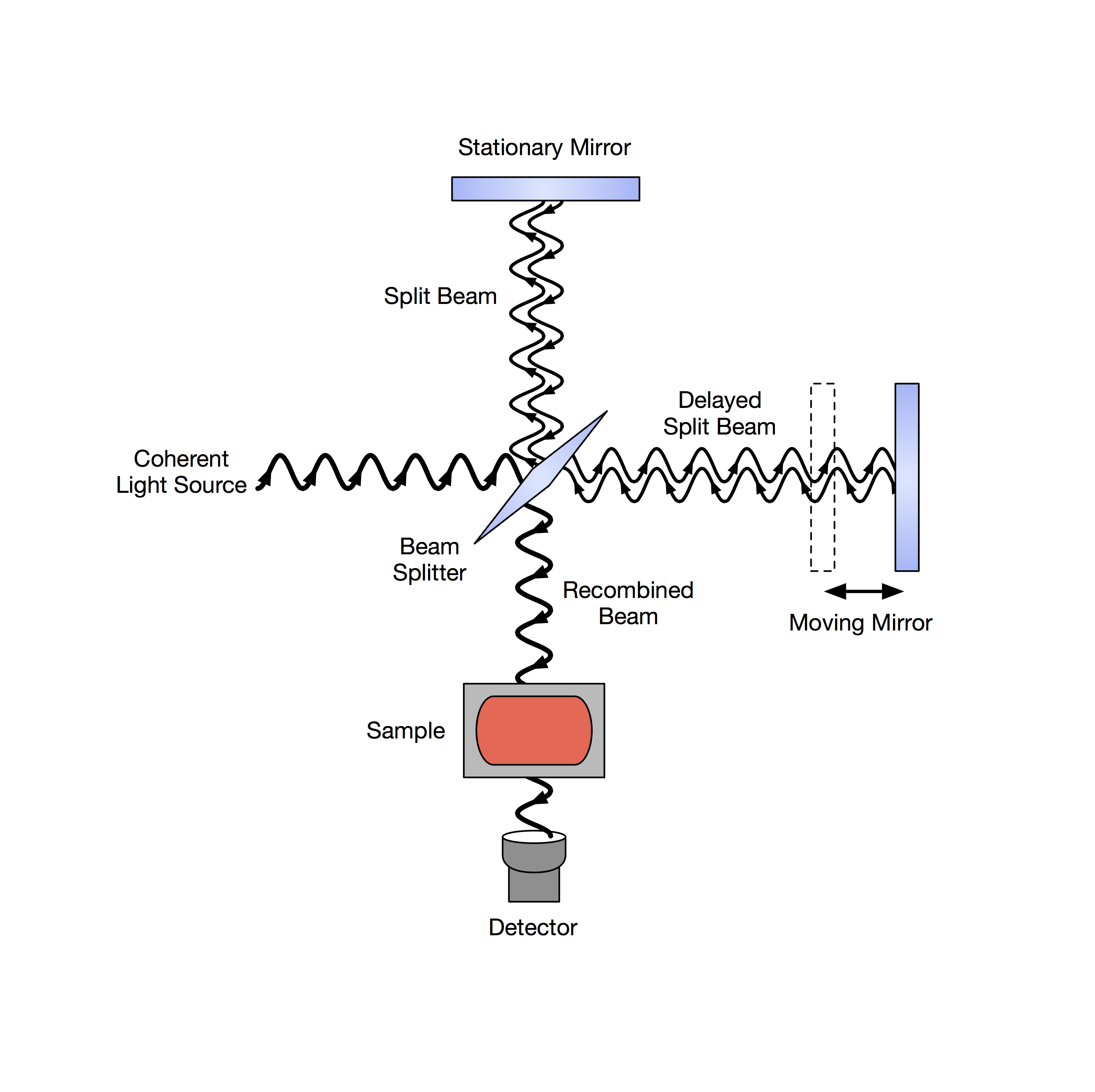
- Fourier Transform Infrared Spectroscopy (FTIR) is commonly used to extract specific information about chemical bonding and molecular structures. It is particularly powerful tool for analyzing organic materials.
- An infrared spectrum represents a fingerprint of a sample with absorption peaks that correspond to the frequencies of vibrations between the bonds of the atoms making up the material. Because each different material is a unique combination of atoms, no two compound produce the exact same Infrared spectrum.
Specifications
- Mid- to Far-IR: 5000-80 cm-1
- Penetration depth: ~1-2 µm
- Sample size: >25 µm
- Full Commercial Spectra Library
Applications
- Identification of all types of organic compounds(solid and liquid) and organic functional groups (chemical bonds)
AFM (Atomic Force Microscope)
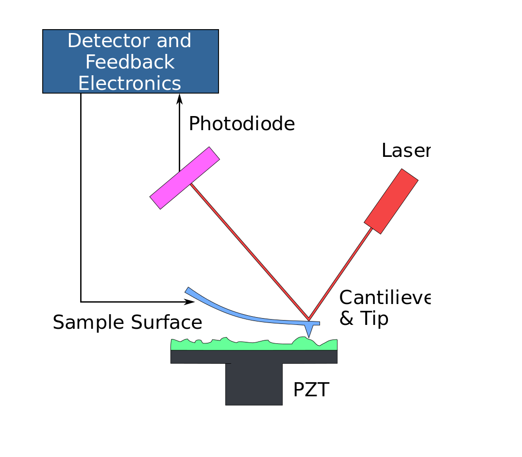
- Atomic Force Microscope (AFM) measures atomic surface topography, which is ideal for characterizing surface roughness at an angstrom scale.
- Besides surface roughness, AFM can provide quantitative measurements of grain size, step height by 3D surface topographic imaging, and capacitance, phase, magnetic field by pitch imaging.
Specifications
- Vertical resolution ~0.1nm
- Best lateral resolution ~7nm
- Maximum scan area 80um x 80 um
- Current range in C-AFM 10pA – 10uA
- Force range in Nanoindentation 1-100uN
Applications
- Surface topology mapping
- Surface roughness measurement
- Electrical current mapping by Conductive Module
- Hardness and Modulus by Nanoindentation Module
EBSD
- Electron backscatter diffraction (EBSD) is a microstructural-crystallographic characterisation technique to study any crystalline or polycrystalline material. The technique involves understanding the structure, crystal orientation and phase of materials in the Scanning Electron Microscope (SEM).
Specifications
- Attached to Helios 600i
- Lateral resolution ~80nm
- Angle resolution ~0.3°
Applications
- Preferred orientation
- Special grain boundary (twin boundary, large angle and small angle boundaries)
- Grain size distribution
AES (Auger Electron Spectroscopy)
- Auger Electron Spectroscopy is a near surface (<5nm) instrument capable of quantifying many elements from a fraction of 1 atomic percent up to 100 percent. It also has better lateral resolution (<10nm) than TOF SIMS, and better surface sensitivity than EDX.
- Elemental Auger mapping is very flexible, and it excels in identifying the composition of small defects and residues.
- Quantified depth profiling through layers can provide both layer composition and interfacial contamination levels.
Specifications
- FEG tip (3-25kV), small sample stage
- CMA detector (all elements except H & He)
- Detection limit: 0.1 to 1.0 atomic %
- SEM: 7nm@20kV; SAM: 10nm@20kV
Applications
- Small size defects down to 20-30nm
- Depth profiling to characterize the contamination
- Element mapping of nano defects
Dual Beam FIB (Focused Ion Beam)
- Focused Ion Beam (FIB) is a versatile analysis technique that can be used to expose hidden defects in a variety of substrates.
- A common application is to prepare samples for TEM analysis using the lift-out technique.
- Another application of FIB is in circuit editing. Electrical connections can be cut and re-routed within the FIB system.
Specifications
- Ga liguid metal ion source, Ga LMIS
- Resolution 5nm at 30kV
- Accelerating voltage 0.5 – 30kV
- Beam current 1.5 pA – 20 nA
- EDX system Oxford Instruments
- EBSD system Oxford Instruments
Applications
- Electro and Ion Beam Imaging
- Micro and Nano Patterning
- Site Specific Cross-sectioning
- Site Specific Deposition
- IC Circuit Editing
- 3D Progressive Milling
- 3D L-Shape Milling
- TEM Sample Preparation
Ion Beam Milling
Specifications
- Argon Ion Beam: 100eV to 6.0 keV
- Cut Width: 0.5 – 5 mm
- Sample Size: 10 X 10 X 4 mm3
- Minimum Sample Temperature: -150°C
Applications
- Large Area Milling & Observation
- Preparation for SEM/EBSD/CAFM
- Delamination and porous cross section
- Delayer
TEM (Transmission Electron Microscope)
- Transmission Electron Microscope (TEM) is a high resolution analysis technique that allows one to see detail on an atomic scale.
- Samples are generally prepared until they are thin enough for electrons to penetrate through it to the detector.
- Coupled with EDX or EELS, quantitative information can be obtained.
- Another application of TEM is to make metrology measurements of crystalline, amorphous, layers, etc.
Specifications
Electron source
- Flexible high tension (20, 40, 80, 120, 160, 200 kV and values in between)
- Schottky field emitter with high maximum beam current (> 100 nA)
- High probe current (0.5 nA or more in 1 nm probe)
Imaging
- TEM point resolution (0.24nm)
- Information limit (0.14nm)
- TEM magnification range 25X-1030kx
- Maximum diffraction angle STEM HAADF resolution (0.19nm)
- STEM magnification range Maximum tilt angle with double-tilt holder + 40°
- EDS solid angle 0.13 srad
- Sample size 10um*4um*100nm(thickness)
Applications
- TEM Imaging and Measurement
- HRTEM Imaging
- EDS Elemental Mapping
- Diffraction analysis and Phase Reconstruction
- Planar View (PV) + Cross Section (XS) TEM
- One Stop Solution
2D/3D X-ray (Industrial CT)
Specifications
- 0.5um recognition resolution
- High power penetration
Applications
- Non-destructive analysis through package
- Wire Bonding integrity
- Die attach delamination
C-SAM
Curve Trace
Specifications
- Reflection and Through scan mode
- 230MHz high frequency transducer
Applications
- Non-destructive analysis through package
- Package delamination
- Stack die delamination
Specifications
- 1pA to 100mA range
- 100uV to 100V range
Applications
- Electrical failure validation
- I-V, C-V
Micro Probing
Deprocessing
Specifications
- 5um prober
- Integrate with test board
Applications
- Electrical failure validation
- Circuit Edit
Specifications
- RIE delayer
- Mechanical delayer
- Chemical delayer
Applications
- Remove Passivation/Metal/Oxide
- Metal short/open
- TEM sample preparation
Chemical Etch
EMMI
Specifications
- Acid etch
- Bas etch
- Solvent
Applications
- Junction stain
- Si dislocation defect
- Epi contamination
Specifications
- InGaAs detector
- Lens 0.8x, 2.5x, 5x, 20x, 50x, 100x
- 12” wafer probe station
- Probe card integration
Applications
- ESD damage localization
- p-n junction leakage
- MOSFET short
- Latch-up localization
- Pressure resistance defect
- Wafer backside analysis
OBIRCH
Thermal
Specifications
- Dual laser 1300nm and 1064nm
- Lens 2.5x, 5x, 20x, 50x, 100x
- 12” wafer probe station
- Digital Lock In function
- Probe card integration
Applications
- Metal open short localization
- ESD damage localization
- p-n junction damage
- Latch-up localization
- Pressure resistance defect
- Wafer backside analysis
Specifications
- InSb detector
- Lens 0.8x, 4x, 8x, 15x
- 12” wafer probe station
- Probe card integration
Applications
- Replacing Liquid Crystal
- Special grain boundary (twin boundary, large
- angle and small angle boundaries)
- Grain size distribution